


- Nucleation-Growth Processes and Morphological Evolution of Polyaniline during Potentiodynamic Polymerization
Eunok Kim†
 , Hyunju Oh, Eonju Lee, and Hyungwook Koo
Department of Chemistry, The University of Suwon, Hwaseoung-si, Gyeonggi-do 18323, Korea
- 변전위법 중합 과정에서 Polyaniline 핵 형성 및 성장 프로세스와 모폴로지 진화
김은옥†
· 오현주 · 이언주 · 구형욱수원대학교 공과대학 융합화학과
The nucleation and growth
processes associated with the morphological evolution of polyaniline during
potentiodynamic polymerization have been investigated. Film deposition was
first ruled by progressive nucleation with a two-dimensional growth process,
and followed by progressive nucleation with a three-dimensional growth process.
Initially, a smooth and compact polyaniline film was deposited on the indium tin
oxide electrode, whereas a fibrous three-dimensional porous network structure
was observed after the initial stage. As the number of cycles increased, the
film became rougher and more porous three-dimensional network structure with
higher free volume, resulting in higher doping levels. Finally, the increased
doping levels and a higher charge carrier mobility lowered the sheet resistance
of the polyaniline film.
변전위법 중합 과정에서 폴리아닐린의 핵 형성 프로세스 및
성장 프로세스를 모폴로지 진화와 연관하여 확인하였다. 필름증착은 초기에 2차원 성장 프로세스를 통한 점진적 핵 형성이 이루어지고, 이어서 3차원 성장 프로세스를 통한 점진적 핵 형성이 지배적이었다. 초기에는, ITO 전극 상에 부드럽고 치밀한 폴리아닐린 필름이 증착되었지만, 초기
단계 후에는 섬유상의 3차원 다공성 네트워크 구조가 관찰되었다. 순환
전압전류의 사이클이 증가함에 따라, 필름은 큰 자유 부피를 가지며 더욱 거칠고 다공성인 3차원 네트워크 구조가 되면서 도핑 레벨이 증가되었다. 결국, 증가된 도핑 레벨과 전하 캐리어 이동성의 향상으로 인해 폴리아닐린 필름의 면저항이 낮아졌다.
In order to understand the nucleation and growth
processes of the polyaniline, their morphological evolution was observed during
the potentiodynamic polymerization, and the effect of polymer morphology on the
electrical conductive properties of the films was investigated.
Keywords: polyaniline, potentiodynamic, nucleation process, growth process, morphology
Conducting polymers are polymers with conjugated p-electrons in a backbone, where the backbone can be
transformed into an electrically conductive structure through a doping process.
Among conducting polymers, polyaniline (PAni) has been widely studied because
of its unique redox chemistry, adjustable electrochemical performance, and
environmental and thermal stability. Moreover, potential applications such as
electrochromic devices, rechargeable batteries, electromagnetic interference
shielding, and sensors have led to extensive research on PAni.1-4
PAni can exist in different forms depending on its degree of oxidation:
pernigraniline (fully oxidized with quinoid imine structures), leucoemeraldine
(fully reduced with benzenoid amine structures), and emeraldine (half-oxidized
with an equal number of imine and
amine structures).5
The doping and de-doping of conducting polymers are reversible processes
that occur almost no degradation of the polymer backbone. The non-redox doping
of conducting polymers is a process in which the number of electrons associated
with the polymer chain is kept constant, resulting in the rearrangement of
energy levels.6 The non-redox doping process in PAni involves the
conversion of non-conducting base form of PAni (PAni-EB) into conducting
emeraldine salt form of PAni (PAni-ES) after treatment with a protonic acid.7
PAni-ES can be obtained through either chemical or electrochemical
polymerization. One of the significant advantages of the electrochemical method
is the ability to deposit a conductive polymer film directly onto electrode
surfaces in a simple and cost effective way, which ensures good ohmic contact
between the electrode and the polymer.8 Furthermore, the
electrochemical method can be used to fine tune the thickness and morphology of
the resulting film by controlling the total charge passed during deposition.3
The three electrochemical deposition methods for PAni are potentiostatic
(constant potential), potentiodynamic (potential scanning or cyclic
voltammetry), and galvanostatic (constant current). We compared the effects of
the deposition method on the morphology and electrochemical properties of PAni,
e.g., potentiodynamic vs. potentiostatic methods, and potentiodynamic vs.
galvanostatic methods.8,9 Upon these previous studies, we proposed a
nucleation and growth processes by observing the morphological evolution of
PAni during the potentiostatic and galvanostatic polymerization, respectively.7,9,10
The nucleation and growth processes provided information at molecular level of
how the polymeric film is generated on the electrode surface, thus enabling the
development
of polymerization strategies to obtain polymer coatings with desired
properties.11 The potentiodynamic polymerization of aniline
involves scanning the potential of the working electrode linearly and
repeatedly, from initial to final values in forward and reverse directions
until the desired amount of polymer has been deposited.
In this work, the resulting PAni films were characterized by scanning
electron microscopy (SEM), Fourier-transformed infrared (FTIR) spectroscopy,
Ultraviolet-Visible (UV-Vis) spectroscopy, and sheet resistance measurements to
get information about the chemical structure, doping level, morphology and
changes in electrical conductive properties as a function of the number of
cyclic voltammetry (CV) cycles. Finally, in order to understand the nucleation
and growth processes of the PAni, their morphological evolution was further
observed during the potentiodynamic polymerization, and the effect of polymer
morphology on the electrical conductive properties of PAni films was
investigated.
Materials. Aniline (≥99.0%,
Duksan Pure Chemicals) was purified by double distillation before use.
Hydrochloric acid (HCl, 37.0%, Duksan Pure Chemicals) and dimethyl sulfoxide
(DMSO, ≥99.0%, Sigma-Aldrich) were used as received.
Potentiodynamic
Polymerization. The PAni films were obtained by cyclic voltammetry for
seven different cycles: 1, 3, 5, 10, 20, 30 and 40, which are denoted for
simplicity as PAni-1cy, PAni-3cy, PAni-5cy, PAni-10cy, PAni-20cy, PAni-30cy and
PAni-40cy, respectively. A three electrode system composed of an ITO working
electrode, Ag/AgCl (3 M NaCl) reference electrode, and platinum plate counter
electrode were used. The PAni film deposited at a scan rate of 10 mV/s and 40
successive cycles of potential between 0.0 and +1.1 V, using a battery
cycler (WON A TECH, WBCS-3000). The experimental temperature was set at
273 K.8,12,13
Characterization. FTIR spectra were
recorded on an FTIR/ATR 4100 Spectrometer (Jasco) in the attenuated total
reflection (ATR) mode for wavenumbers of 600-2000 cm−1. UV-Vis
spectra were recorded on an S-3100 Spectrophotometer (Scinco) for the
wavelengths of 250-1100 nm. High-resolution scanning electron microscopy (SEM)
imaging was performed using a LYRA 3 (Tescan) system. The thickness of the
films was measured using a micrometer caliper. The four-point probe 2401 Source
Measurement Unit (Keithley) was used to measure the sheet resistance of the
films. In the case of the 1, 3 and 5 cycles, the thickness of the film was not
thick enough for the measurement, so FTIR spectroscopy, UV-Vis spectroscopy,
and sheet resistance measurements could not be performed.
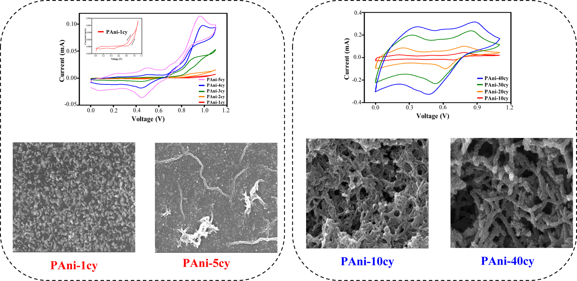
The nucleation and growth processes of conducting polymers involve
several stages, beginning with the oxidation of the monomer at the anode
followed by oligomerization and polymerization.1,14 Figure 1 shows
the cyclic voltammetric behavior for the polymerization of aniline during the
first five successive cycles.
As shown in the first cycle (inset of Figure 1), a significant increase
in anodic currents starts at about +0.90 V and corresponds to the
oxidation of aniline, which is considered to be the rate-determining step.5
The trace crossing, which appears as an anodic current observed on the reverse
sweep of the first cycle, could result from slow follow-up reactions occurring
at the diffusion layer in the vicinity of the electrode surface.3
The oxidation of aniline results in the formation of PAni nuclei on the ITO
surface, leading to the formation of oligomers that subsequently turn into the
polymer after successive potential cycles.15 The cyclic voltammogram
shows that the current increases in each successive cycle, confirming the
deposition of PAni. As the potential of the working electrode changes with
successive potential cycles, the deposited PAni changes between its
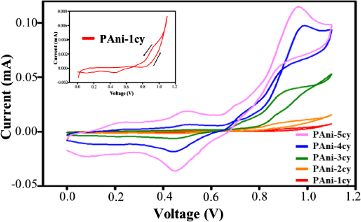
non-conducting (de-doped) and conducting (doped) forms. Figure 2 shows the
cyclic voltammetric behavior recorded at different cycles (10, 20, 30, and 40)
during the polymerization of aniline. An increase in current is observed for
each consecutive cycle, which indicates a steady growth in the thickness of the
polymer film. Therefore, the thickness of the PAni film can be controlled by
changing the number of cycles. Typical PAni CV curves exhibit two pairs of
redox peaks, which are accompanied by charge transfer and mass transport. The
first pair of redox peaks at the lower positive potential corresponds to the
leucoemeraldine/polaronic emeraldine transition. The second pair of redox peaks
at the higher potential corresponds to the polaronic emeraldine/pernigraniline
transition.9 The anodic and cathodic currents increase rapidly with
increasing cycle number because PAni has good catalytic activity to aniline.
Such activity, in turn, promotes
polymer deposition on the surface
of the electrode and is therefore regarded as an autocatalytic process.16
This result further shows that as the PAni layers grow on the ITO electrode
with increasing the number of cycles, in which the actual electrode surface
area gradually increases. The anodic peaks shift towards the positive
direction, and the cathodic peaks shift towards the negative direction while
simultaneously increasing the current. This shifting in peak potentials is
consistent with the ohmic contribution to the overpotential.17 Ohmic
overpotential in an electrochemical cell is associated with both the ionic and
electronic resistance, as well as contact resistance between all components.
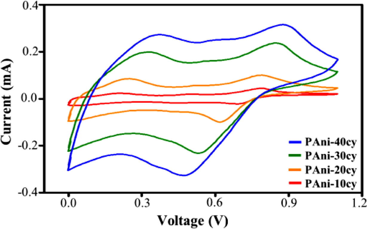
FTIR spectroscopy in ATR mode is a powerful technique for analyzing the
chemical structure of PAni film, and in particular, the oxidation state of its
chains. Figure 3 shows the FTIR spectra of PAni obtained for different cycle
numbers (10, 20, 30, and 40). Some low intensity peaks at ~620, ~680, and
~790 cm−1 are ascribed to C-H bond vibrations in the benzenoid
rings.18 The characteristic band at ~1565 cm−l
arises mainly from both the C=N and C=C stretching vibrations of the quinoid
ring, while the band at ~1490 cm−l is attributed to the C-C
stretching vibration of the benzenoid ring. These bands are essential for the
characterization of PAni as they provide information concerning its redox
state. The band at ~1290 cm−1 corresponds to the C-N stretching
in the secondary aromatic amine, and its high intensity indicates the presence
of long conjugated length along the polymer chains.18 The typical
band at ~1250 cm−l is related to the C−N•+ stretching
vibration in the conducting form. The strong band at ~1140 cm–1
is attributed to the C–H aromatic in-plane bending vibration, which could be
described as an “electronic-like band,” demonstrating a fully doped conducting
PAni. The intensity ratio of quinoid (Q) to benzenoid (B) structures (IQ/IB)
can be used to estimate the oxidation state of PAni.18,19 The (IQ/IB)
ratio for PAni-10cy was 0.89, indicating that there are more benzenoid units
within the polymer. The (IQ/IB) ratio value
of ~1.0 for PAni-20cy, PAni-30cy, and PAni-40cy indicates a conducting form for
the emeraldine oxidation state of PAni.
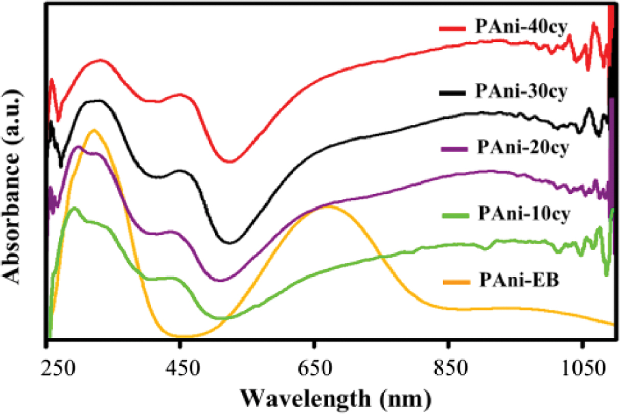
UV-Vis spectroscopy provides information on the electronic transitions
between energy bands formed by p-conjugation along
the polymer backbone. Figure 4 shows the UV-Vis absorption spectra of PAni-EB
and conducting PAni obtained at different cycle numbers (10, 20, 30, and 40),
which are dissolved in DMSO. HCl-doped PAni was de-doped using sodium hydroxide
to obtain PAni-EB. The UV-Vis spectrum of de-doped PAni-EB shows two
characteristic absorption bands at ~330 and ~650 nm, which can be assigned to
the p–p* transition of the
benzenoid rings and the excitation absorption of the quinoid rings,
respectively. The doping process of conducting polymers introduce charge
carriers (polaron and bipolaron) into the polymer and renders it conductive,
leading to a change in its UV-Vis absorption spectrum.10 Upon
doping, the quinoid transition at ~650 nm disappears, and two new absorption
bands appear. These new absorption bands are attributed to the bipolaron and
polaron transitions at ~450 and ~780 nm, respectively.20 The
decrease in absorbance at ~650 nm indicates that the imine nitrogen atoms
of the quinoid rings are converted to benzenoid rings by protonation with the
HCl dopant, which can be attributed to the steric effect of dopant anions. As
the number of cycles increases from 10 to 40, a red-shift of the p–p* transition is
observed for the 304 nm and 336 nm bands, demonstrating a smaller energy
gap.19 Previous research showed that, with increase of the doping
level, the absorption at ~650 nm decreases while that of the ~780 nm increases.7,10
A broad absorbance at wavelengths greater than ~800 nm is related to the
presence of free carrier tails, which is associated with an increased
delocalized polaron band. As the conjugation length gets longer, the band
shifts to broader wavelengths and becomes extremely large.20 The
doping level can be roughly estimated from the absorption spectra using the
relative intensity ratio of absorbance at ~780 nm (p–polaron
transition) and ~330 nm (p–p* transition).21 The measured relative
intensity ratios (I~780/I~330) were 0.72,
0.88, 0.97, and 0.99 for the 10, 20, 30, and 40 cycles, respectively. The
highest (I~780/I~330) ratio observed for
PAni-40cy indicates that as the number of cycles increases, it becomes easier
for the counter ions to diffuse into the film, yielding higher doping levels.
The electrodeposition of PAni involves both nucleation and growth
processes, beginning with the formation of PAni nuclei on the surface of the
electrode and followed by their subsequent growth.14,22
Instantaneous nucleation and progressive nucleation are two types of nucleation
processes. In instantaneous nucleation, nearly all nuclei are formed
simultaneously, while in progressive nucleation, nuclei are continually
generated throughout the polymerization process.1,23 There are three
types of growth processes: one-dimensional (1-D), two-dimensional (2-D) and
three-dimensional (3-D). The 1-D growth process refers to growth in only one
direction, perpendicular to the electrode surface. In 2-D growth,
the nuclei preferably grow parallel to the electrode, and 3-D growth
implies similar growth rates in both perpendicular and parallel directions.1,24
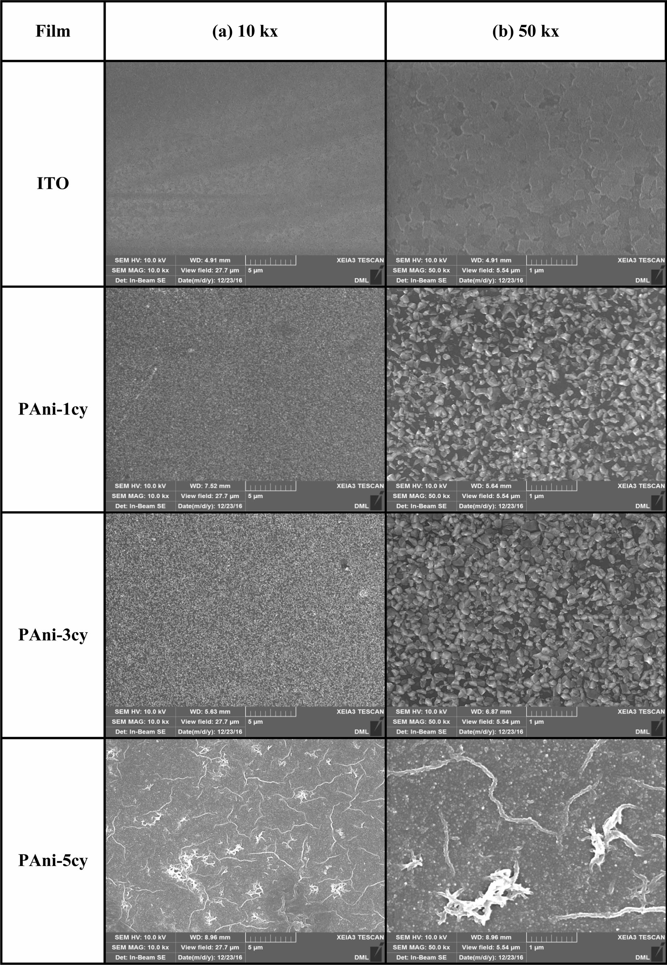
The morphological variation of PAni during its growth process is shown in
Figures 5 and 6. SEM images were acquired at magnifications of (a) 10 kx and
(b) 50 kx. Figure 5 shows SEM images of ITO and PAni obtained at different
cycles (1, 3, and 5). The significant differences between the images of ITO and
PAni-1cy indicate that deposition begins in the first cycle. Initially, aniline
radical cations (“oxidized species”) generated at the beginning of monomer
oxidation are adsorbed onto the surface of the ITO in the first cycle, and the
particles start to cover the ITO surface. No significant morphological changes
were observed in the third cycle as compared to the first one, though the ITO
surface was more compactly coated with the particles in the third cycle. The
smooth and compact PAni film
formed on the ITO surface
indicates a predominance of progressive nucleation with a 2-D growth process.25
In the fifth cycle, further nucleation occurs and a second layer begins to form
on the first 2-D layer. Given that the doping of conducting polymers occurs
after polymer formation, and that the process of film growth is faster than the
doping process, it is difficult for the dopant counter ions to penetrate the
film due to the lack of free volume, resulting in a low doping level for PAni.21
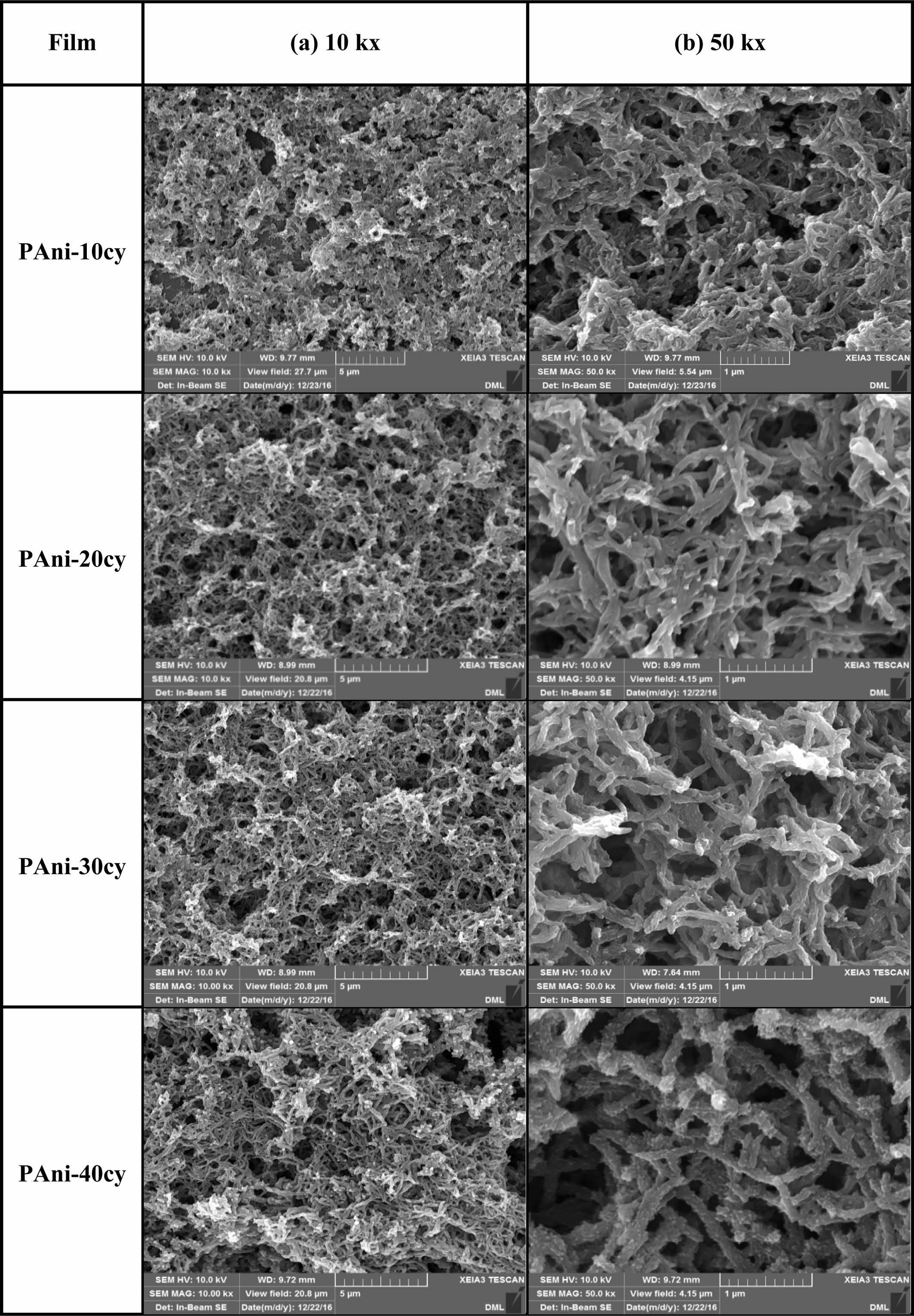
Figure 6 shows SEM images of PAni obtained at different cycles (10, 20, 30, and
40). As the number of cycles increases, the film becomes thicker due to
sequential layer-by-layer deposition. The newly formed layer on top of the
first compact layer shows an interconnected fibrous 3-D network structure after
ten cycles. This fibrous morphology is inconsistent with Heinze’s finding that
cyclic voltammetry favors the formation of disordered chains and open
structures.1 According to our previous studies, the fibrous porous
structure is likely related to the effects of the ingress and expulsion of
counter ions during each redox cycle, promoting the rearrangement of the
polymeric structure.8 After the initial stage, the deposition of
PAni was gradually governed by progressive nucleation with a 3-D growth
process. As the number of cycles increases, the fiber thickness increases and
the film adopts a rougher and more porous 3-D network structure. As a result,
the diffusion of counter ions into the film becomes easier and the doping level
is enhanced by the formation of the porous crosslinked 3-D interpenetrating
polymer network.21,26 In conclusion, the deposition of PAni
initially occurs via progressive nucleation with a 2-D growth process, followed
by progressive nucleation with a 3-D growth contribution. Thus, the number of
CV cycles plays an important role in determining the morphology of the polymer
and may affect the electrochemical properties of PAni.
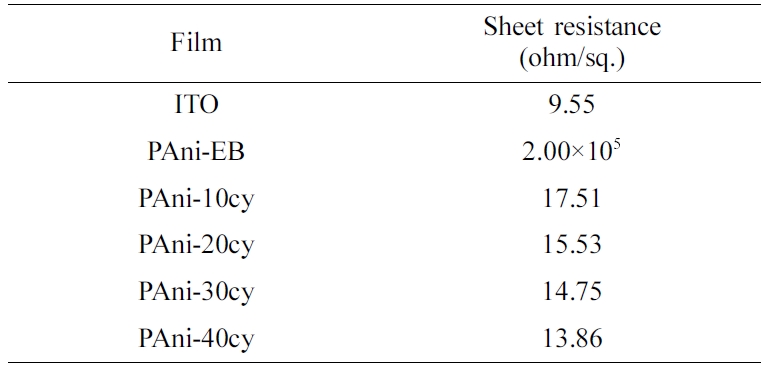
Two-point probe methods are typically used for sheet resistance
measurements. However, when the measured resistance is relatively low,
four-point probe (e.g., van der Pauw) measurements are utilized as this allows
for the elimination of the influence of contact resistance at the
current-carrying electrodes. When the number of cycles increases, the lower
part of the film deposited on the ITO surface becomes thicker than the upper
part of the film as the influence of gravity becomes increasingly important.
Therefore, four-point probe measurements were performed at five different
locations, and the average of the measured values was used.
For cycles 1, 3, and 5, the sheet resistance was not measured as the films were
too thin to allow for reliable values. Table 1 shows the sheet resistances of
ITO, PAni-EB, and PAni films obtained for different cycles (10, 20, 30, and
40). As the number of cycles increased, sheet resistance gradually decreased and
electrical conductivity increased. As mentioned above, doping of the conducting
polymers introduce charge carriers into the polymer chains that are balanced by
counter ions. Since the charge carriers generated by the doping process are
delocalized and provide the primary source of conduction in protonic acid doped
conducting polymers, the conduction mechanism is complicated.27 As
expected, increasing doping levels yield an increase in electrical conduction
and reduce the sheet resistance due to the formation of a porous crosslinked
3-D network between the polymer chains and the dopant counter ions. In general,
charge carrier mobility along a polymer chain (intra-chain) is higher than the
mobility of charge carriers hopping between adjacent chains (inter-chain).
Therefore, the thicker chain alignment in the PAni-40cy enhances charge carrier
transport along the polymer chains, affecting its macroscopic electrical
conduction. In conclusion, the conduction mechanism is affected by the doping
level and the conformational changes in the polymer chains and relies on both
the intra-chain movement of charge carriers along polymer chains and the
inter-chain charge transport between adjacent chains.28,29
|
Figure 1 Cyclic voltammetric behavior of aniline polymerization for the first five successive cycles (Inset: first cycle). |
|
Figure 2 Cyclic voltammetric behavior recorded at different cycles (10, 20, 30, and 40) during the polymerization of aniline. |
|
Figure 3 FTIR spectra of PAni obtained for d ifferent cycle numbers (10, 20, 30, and 40). |
|
Figure 4 UV-Vis spectra of PAni-EB and PAni obtained for different cycle numbers (10, 20, 30, and 40). |
|
Figure 5 SEM images of ITO and PAni obtained for different cycle numbers (1, 3, and 5). |
|
Figure 6 SEM images of PAni obtained for different cycle numbers (10, 20, 30, and 40). |
|
Table 1 Sheet Resistance of ITO, PAni-EB, and PAni Films Obtained for Different Cycle Numbers (10, 20, 30, and 40) |
Understanding nucleation and growth processes can provide critical insight into the
formation mechanisms of PAni films on the electrode surface, allowing for the
development of polymerization strategies for PAni deposition with desired
electrochemical properties. In this work, the nucleation and growth processes
associated with the morphological evolution of PAni during potentiodynamic
polymerization were investigated. Cyclic voltammograms were recorded during the
potentiodynamic growth of PAni films. Initially, progressive nucleation with a
2-D growth process predominated, followed by progressive nucleation with a 3-D
growth process. The chemical structure, doping level, and morphology of PAni
were found to be determined by the electrochemical properties of the films. The
electrical conductance of PAni films could be controlled by modifying the
polymer morphology.
- 1. J. Heinze, B. A. Frontana-Uribe, and S. Ludwigs, Chem. Rev., 110, 4724 (2010).
-

- 2. A. Kellenberger, D. Ambros, and N. Plesu, Int. J. Electrochem. Sci., 9, 6821 (2014).
- 3. N. H. Khdary, M. E. Abdesalam, and G. El Enany, J. Electrochem. Soc., 161, 63 (2014).
-
- 4. H. J. N. P. D. Mello and M. Mulato, Synth. Met., 239, 66 (2018).
-
- 5. Y. Jafari, S. M. Ghoreishi, and M. Shabani-Nooshabadi, Synth. Met., 217, 220 (2016).
-
- 6. T. H. Le, Y. Kim, and H. Yoon, Polymers(Basel), 9, 150 (2017).
-
- 7. E. Kim and J.-H. Kim, Bull. Korean Chem. Soc., 38, 850 (2017).
-
- 8. E. Kim, N. Kang, J. J. Moon, and M. Choi, Bull. Korean Chem. Soc., 37, 1445 (2016).
-
- 9. E. Kim and M. Choi, Polym. Korea, 40, 728 (2016).
-
- 10. E. Kim and J. Lee, Polym. Korea, 42, 834 (2018).
-
- 11. M. Romero, M. A. Del Valle, R. del Río, F. R. Díaz, and F. Armijo, Int. J. Electrochem. Sci., 7, 10132 (2012).
- 12. E. Lee and E. Kim, Bull. Korean Chem. Soc., 34, 1 (2013).
- 13. E. Kim, J. Korean Chem. Soc., 59, 423 (2015).
-
- 14. M. Romero, M. A. Del Valle, R. del Río, F. R. Díaz, F. Armijo, and E. A. Dalchiele, J. Electrochem. Soc., 160, 125 (2013).
-
- 15. D. Sazou, M. Kourouzidou, and E. Pavlidou, Electrochim. Acta, 52, 4385 (2007).
-
- 16. L. Shen and X. Huang, Synth. Met., 245, 18 (2018).
-
- 17. G. Das and H. H. Yoon, Int. J. Nanomedicine, 10, 55 (2015).
-
- 18. F. F. Fang, Y. Z. Dong, and H. J. Choi, Polymer(Guildf), 158, 176 (2018).
-
- 19. J. Zhao, Z. Qin, T. Li, Z. Li, Z. Zhou, and M. Zhu, Prog. Nat. Sci. Mater. Int., 25, 316 (2015).
-
- 20. N. Karaoğlan and C. Bindal, Eng. Sci. Technol. Int. J., 21, 1152 (2018).
-
- 21. C. Liu, J. Zhang, G. Shi, and F. Chen, J. Appl. Polym. Sci., 92, 171 (2004).
-
- 22. S. Mu and Y. Yang, J. Phys. Chem. B, 112, 11558 (2008).
-
- 23. W. Huang, J. Li, and Y. Xu, Materials(Basel), 10, 1205 (2017).
-
- 24. M. M. Gvozdenović, B. Z. Jugović, J. S. Stevanović, and B. N. Grgur, Hem. Ind., 68, 673 (2014).
-
- 25. Q. Qin, F. He, and W. Zhang, J. Nanomater., 2016, 1 (2016).
- 26. M. Massi, C. Albonetti, M. Facchini, M. Cavallini, and F. Biscarini, Adv. Mater., 18, 2739 (2006).
-
- 27. E. Song and J.-W. Choi, Nanomaterials, 3, 498 (2013).
-
- 28. N. Bohli, F. Gmati, A. B. Mohamed, V. Vigneras, and J. L. Miane, J. Phys. D. Appl. Phys., 42, 205404 (2009).
-
- 29. J. A. L. Sánchez, A. M. Díez-Pascual, R. P. Capilla, and P. G. Díaz, Polymers(Basel), 11, 1032 (2019).
-
- Polymer(Korea) 폴리머
- Frequency : Bimonthly(odd)
ISSN 0379-153X(Print)
ISSN 2234-8077(Online)
Abbr. Polym. Korea - 2023 Impact Factor : 0.4
- Indexed in SCIE
 This Article
-
2020; 44(3): 369-376
Published online May 25, 2020
- 10.7317/pk.2020.44.3.369
- Received on Feb 14, 2020
- Revised on Mar 15, 2020
- Accepted on Mar 16, 2020
Services
Shared
Correspondence to
- Eunok Kim
-
Department of Chemistry, The University of Suwon, Hwaseoung-si, Gyeonggi-do 18323, Korea
- E-mail: eokim@suwon.ac.kr
- ORCID:
0000-0003-0344-0872
Hyecheon Building(Room 601), #354, Gangnam-Daero, Gangnam-Gu, Seoul 06242, Korea
TEL : 82-2-568-3860, 561-5203, 569-3860 FAX : 82-2553-6938 E-mail: polymer@polymer.or.kr