- A Transparent Cyanated Polyimide Gate Dielectrics for High Performance Organic Field-Effect Transistors
Yonghwa Baek#, Xinlin Li*,#, Prerna Chaudhary**, Chan Eon Park, Sung Soo Han**,†, Tae Kyu An***,†
 , and Se Hyun Kim**,†
Polymer Research Institute, Department of Chemical Engineering, Pohang University of Science and Technology (POSTECH), Pohang 37673, Korea
*Department of Mechanical Engineering Science, Yeungnam University, Gyeongsan 38541, Korea
**School of Chemical Engineering, Yeungnam University, Gyeongsan 38541, Korea
***Department of Polymer Science & Engineering and IT Convergence, Korea National University of Transportation, 50 Daehak-Ro, Chungju 27469, Korea- 고성능 유기전계효과 트랜지스터 구현을 위한 시아노기가 도입된 투명 폴리이미드 절연층 개발
백용화# · Xinlin Li*,# · Prerna Chaudhary** · 박찬언 · 한승수**,† · 안태규***,†
 · 김세현**,†
포항공과대학교 화학공학과, *영남대학교 엔지니어링사이언스학과, **영남대학교 화학공학부 ***한국교통대학교 나노화학소재공학과 & 정보기술융합학과
Polyimides are attractive choices for the formation of films in various industries due to their excellent mechanical, thermal, and chemical stabilities. However, the insolubility of their precursors (poly(amic acid); PAA) and the intrinsically poor optical transmittance of polyimide films have impeded their applications in various fields. In this study, we present newly synthesized cyanated polyimide gate dielectrics, poly(2-cyano-p-phenylene pyromellitimide) (cy-PPI), and applied them to organic field-effect transistors (OFETs). The strongly electron-withdrawing cyano groups of PAA played a critical role in improving the solubility and transparency of the polyimide. The solution-processed cy-PPI films exhibited good dielectric properties, and their smooth surfaces led to a better crystalline morphology in the pentacene film grown over their surfaces. As a result, the good electrical properties (0.15 cm2/Vs of field-effect mobility and 1.2×10⁵ of on/off ratio) were achieved for the pentacene-based cy-PPI OFETs.
폴리이미드는 대부분의 고분자 필름의 단점으로 지적되고 있는 열적, 화학적 취약성을 극복할 수 있는 좋은 재료이다. 이렇게 우수한 특성에도 불구하고, 폴리이미드는 전구체인 폴리아믹산의 낮은 용해도로 인해 가공성이 좋지 않을 뿐만 아니라, 특유의 황토빛을 띠는 성질로 인하여 디스플레이 분야로의 응용이 제한적이다. 본 연구에서는 폴리아믹산의 디아민 단량체에 시아노기(-CN)를 도입하여, 폴리이미드의 우수한 내화학성, 내열성, 전기적특성을 그대로 지니면서도 전자 전이 복합화에 의해 황토색 빛을 띠는 현상을 극복하여 무색 투명한 형태를 띠는 폴리이미드 필름인 poly(2-cyano-p-phenylene pyromellitimide; cy-PPI)를 제조하고 유기전계효과 트랜지스터의 절연층으로 적용시켜보았다. cy-PPI 박막은 우수한 절연특성을 보여주었을 뿐만 아니라, 그 위에서 반도체 결정이 잘 성장하게 해주었다. 그 결과, cy-PPI 절연층이 도입된 펜타센 트랜지스터 소자에서 0.15 cm2/Vs의 전하이동도와 1.2×10⁵의 점멸비의 우수한 전기적 성능을 나타내었다.
Keywords: organic field-effect transistors, gate dielectrics, polyimide, cyano groups
This work supported by a National Research Foundation of Korea (NRF) grant funded by the Korean government (MSIP) (No. 2017R1C1B2002888), and was also supported by Yeungnam University Research Grants in 2018.
The advent of organic electronics has marked a new era in modern society because of their advantageous properties, in particular their flexibility1,2 as well as low cost and large-area solution processability.3 They have significantly contributed to the improvement of already existing device technologies and the development of emerging ones, including displays, electronic circuits,4 energy harvesting,5 sensors,6 actuators, and so on. Among the organic electronic devices, organic field-effect transistors (OFETs) have received intensive attention as unit switching devices in the above-mentioned electronic applications. Although the performance levels of state-of-the-art OFETs are comparable to or surpass those of amorphous Si or oxide semiconductors, several issues regarding OFETs remain to be addressed before they can be fully commercialized.
The gate dielectric layer plays a significant role in the operation of OFETs because the conducting channel is formed at the interface between the semiconductor and gate dielectric layer.7 Note that the key device performances such as fieldeffect mobility, threshold voltage (Vth), and subthreshold slope (SS) are subject to the interface properties: the crystalline morphology of the semiconductor (crystallinity and molecular orientation) and the surface roughness and functionalities of the gate dielectric layer, which can control the trap density and hence enable the capture of free charge carriers in the conducting channel. In particular, the growth of organic semiconductors is influenced by the surface properties (surface energy and roughness), and hence the properties of the gate dielectric are regarded as one of the critical factors that determine device performance. In addition, operation issues of OFETs (operating voltage, leakage current, and hysteresis) are largely determined by the bulk properties of the gate dielectric, such as dielectric constant and dielectric strength, as well as dielectric relaxation. Inorganic oxide gate dielectrics (such as SiO2, Al2O3, ZrO2, TiO2, and HfO2) have been widely used as gate dielectric layers for high-performance OFETs due to their relatively high dielectric constants and excellent dielectric strength levels.8 However, the rigidness and complicated processing of inorganic oxide gate dielectric layers can limit the expansion of OFETs to flexible and stretchable electronic applications. Furthermore, the surfaces of these dielectric layers are highly polar due to the presence of hydroxyl groups, which leads to the creation of interface traps and disturbs the crystal growth of organic semiconductor molecules.9 Therefore, to reduce the surface polarity, the surface of the inorganic oxide film should be treated with a hydrophobic layer such as a self-assembled monolayer (SAM) or polymer film.10
Polymer materials have garnered considerable attention as alternative gate dielectric materials for OFETs.11 They can be easily solution-deposited on substrates in mild conditions (low temperature, ambient pressure). In addition, polymer films are applicable to other organic materials as well as all parts of substrates, and their chemical structures are unlimited.12 Many polymer gate dielectrics, for example, polystyrene (PS),13 poly(vinylalcohol) (PVA),14 poly(4-vinylphenol) (PVP),15 poly (methylmethacrylate) (PMMA),16 and poly(perfluorobutenylvinylether) (CYTOP),17 have been reported. However, most polymers have shown vulnerability to several factors such as structure, heat, water, and chemicals. On the other hand, polyimides (PIs) have been shown to exhibit excellent resistance to heat and a wide range of organic solvents by virtue of their strong imide backbones,18 thereby providing a great potential for use as gate dielectric materials in solution-processable OFETs.
Nevertheless, PI films have suffered from critical issues, in particular insolubility and poor optical transmittance. In general, the precursor of PI, poly(amic acid) (PAA), has not been readily dissolved in common solvents.19 For this reason, the application of solution-processed OFETs with PI gate dielectrics has been hindered. In many previous reports, several approaches for increasing the solubility of PAA have been introduced, such as incorporation of a flexible linkage or bulky substituents into the PI backbones, and use of non-coplanar or alicyclic monomers. These approaches have led to an increase in the solubility of PAA by reducing the extent of the interactions between the PI chains.20 On the other hand, deep coloration greatly limits the widespread application of the PI films in areas where transparency and colorlessness are the basic needs.21 Conventional PI films have generally suffered from the deep colors and poor optical transmittance originated from the formation of charge-transfer complexes (CTCs) in their highly conjugated molecular structures.22 Such CTCs trigger excitation of pi electrons in the PI films, and these films then can gradually absorb visible light. Therefore, excellent optical properties of PI films can be achieved by introducing the inductive effect of strong electron-withdrawing groups such as trifluoromethyl (-CF3)23 or sulfonyl (-SO2) groups,24 which have been indicated to obstruct the dense chain stacking and to break the electron conjugation, and consequently, significantly restrain the formation of inter- and intra-molecular CTCs.
In this paper, we synthesized new PI films, ones displaying good transmittance of visible light and solubility in organic solvents, and have applied these films as gate dielectrics to OFETs. The molecular stiffness, high polarity and strong intermolecular interactions of typical PI make them virtually insoluble in any organic medium, which causes difficulties in processing. Fortunately, we were able to effectively enhance PI solubility to a sufficient level by introducing cyano groups into its main chain. These cyano groups allowed for the formation of a smooth gate dielectric surface by spin-coating, and an overlying vacuum-deposited semiconductor formed a favorable crystal morphology. Moreover, the strong electronwithdrawing cyano groups apparently generated a local electric field that accumulated holes. The accumulated holes provided additional mobile carriers and resulted in an increased field-effect mobility. As a result, our devices showed good electrical performances, with a hole mobility of 0.15 cm2/Vs, threshold voltage (Vth) of -5.02 V, on/off ratio of 1.2×10⁵, subthreshold slope (SS) of 1.94 V/decade, and negligible hysteresis compared to those of PVP gate dielectric-based
OFETs.
Material Synthesis. The 2-cyano-1,4-phenylene diamine (cy-PPD) was purchased from Kolon Industries, and 1-methyl- 2-pyrrolidinone (NMP) and pyromellitic dianhydride (PMDA) were purchased from Sigma Aldrich. Cy-PPD and PMDA were purified by sublimation under high vacuum twice. Equimolar amounts of cy-PPD and PMDA were dissolved in NMP to a concentration of 10 wt%. The mixed solution was stirred for 10 h at 0.5 ℃ under a nitrogen atmosphere. Then, a PAA solution was finally obtained.
Fabrication of the OFETs. A heavily n-doped silicon (Si) wafer was used as a gate electrode and substrate. It was cleaned with a piranha solution, then ultra-sonicated and rinsed with distilled water, and finally treated with UV-ozone. PAA and poly(4-vinylphenol) (PVP) were spin-coated on the cleaned Si substrate at 2500 and 5000 rpm, respectively, using dimethylformamide (DMF) as the solvent. The as-spun PAA film was subjected to thermal annealing at 200 ℃ for 2 h, and was as a result converted to a PI film (with a thickness was 280 nm). 50 nm thick pentacene layers were deposited on the gate dielectrics via a vacuum pr℃ess (deposition rate: 0.1- 0.2 Å/s, vacuum pressure: -10–6 Torr, substrate temperature: 25 ℃). A 100-nm-thick gold electrode was deposited on the pentacene semiconductor layers by carrying out thermal evaporation through a metal shadow mask. The channel length (L) and width (W) values of the mask were 150 and 1500 μm, respectively.
Device Characterization. The surface energy (γs) of the PI film was calculated by measuring the contact angle using two test liquids (DI water and diiodomethane). The γs values were calculated according to the eq. (1)

by fitting the eq. (1) to the measured contact angle values (Table 1). In the eq. (1), γlv is the surface energy of the liquid and the superscripts d and p refer to the dispersive and polar components, respectively. The surfaces of the PI and pentacene films were characterized by atomic force microscopy (AFM) in tapping and ScanAsyst modes (Bruker Nanoscope). Twodimensional grazing-incidence X-ray diffraction (XRD) experiments were performed at the 5A beamline (wavelength = 0.1071 nm) of the Pohang Accelerator Laboratory (PAL). The capacitance and leakage current density were characterized by fabricating a metal–insulator–metal (MIM) capacitor via the thermal deposition of gold onto the PI or PVP/heavily doped Si substrate. The measurements were taken using an Agilent 4284 precision LCR meter. Transfer and output characteristics of the OFETs were measured using a Keithley 4200 SCS unit in a N2-purged glove box (the concentrations of H2O and O2 were maintained at less than 0.1 ppm). Threshold voltage (Vth) was calculated from the transfer curve in the saturation regime swept over the gate voltage range VG = +10 to –30 V.
|
Table 1 Surface and Dielectric Properties of PVP and cy-PPI Gate Dielectric Layers |

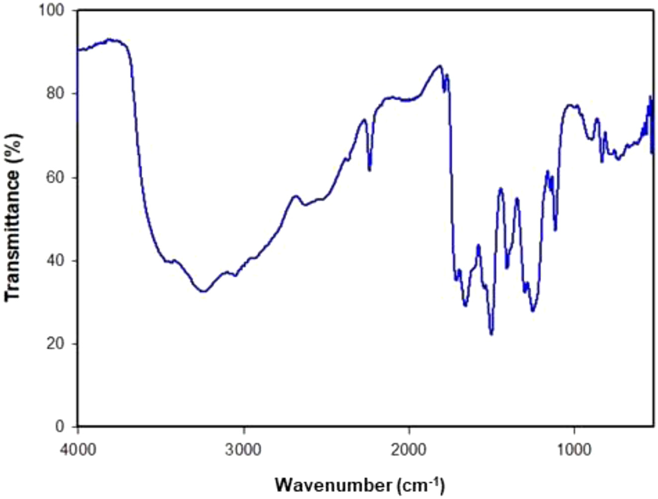
Material Preparation. The synthesis of the PAA, presented in Figure 1, was accomplished by carrying out addition polymerization under N2 atmosphere. The identity of the obtained polymer was confirmed by FTIR and 1H NMR spectra as shown in Figure 2 and 3.
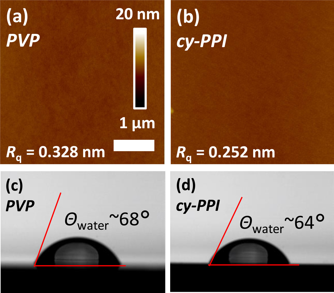
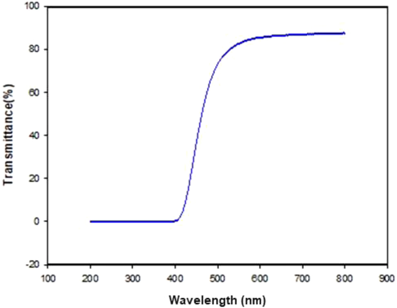
Film Characterization. To investigate surface properties of the gate dielectric layers, poly(2-cyano-p-phenylene pyromellitimide) (cy-PPI) and PVP (conventional polymer gate dielectric for OFETs) were prepared. Figure 4 and Table 1 show the surface properties of the cy-PPI and PVP films. First, the surface energy of the gate dielectric was measured by using two test liquids (DI water and diiodomethane). The water contact angle and surface energy of the cy-PPI film were 64° and 49.32 mJ/m2, similar to that of pentacene (42-48 mJ/m2). Cy- PPI gave a very smooth surface (root-mean-square (RMS) of 0.252 nm). The PVP surface showed an RMS of 0.328 nm. That is, the two different films exhibited very similar surface roughness levels. In bottom-gate OFETs, rough gate dielectric surfaces have been shown to impede the lateral diffusion of pentacene molecules, hence leading to smaller grain sizes.25 It may lead to a degradation of electrical performance in OFETs by blocking the flow of carriers from the source to drain electrode. Based on these results, we expected cy-PPI-based devices to exhibit good electrical performances. Furthermore, our cy-PPI film showed transmittance values of over 80% in the wavelength range between 500 and 800 nm, and over 90% in the wavelength range between 600 and 900 nm. (see Figure 5), i.e., it showed much better transparency than has the Kapton PI film.
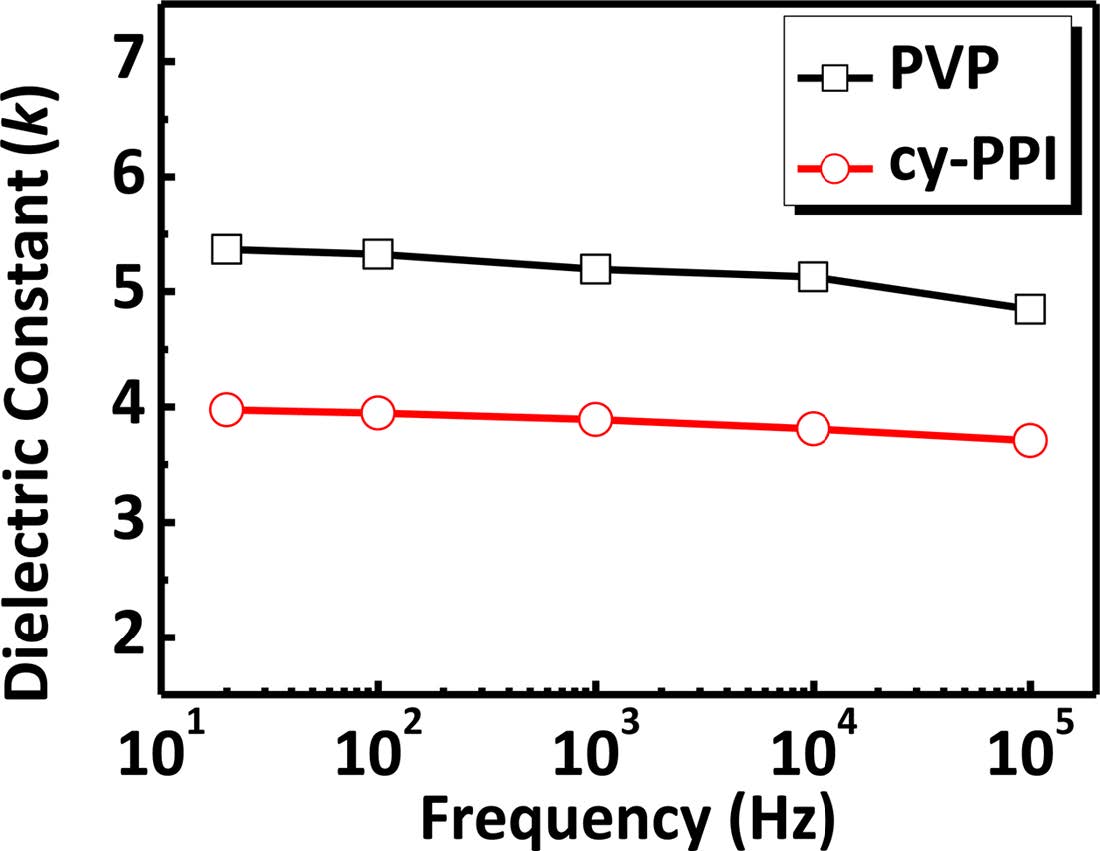
Dielectric Characterization. To characterize the dielectric bulk properties, we fabricated metal-insulator-metal (MIM) structures by sandwiching 280-nm-thick polymer layers between the gold electrode and Si substrate. Capacitance (C), corresponding to the amount of charge stored in a gate dielectric at a specific voltage, is defined by C = kε0A/d, where ε0 is the permittivity of free space, A is the area of the capacitor, and d is the thickness of the gate dielectric. Capacitance was measured at various frequencies to investigate its stability. If capacitance is changed, the semiconductor may operate in a different regime and the density of carriers in the channel may be changed. That is to say, the drain current in the OFET may be influenced by capacitance. Therefore, a low frequency dependence is desired for stable OFET operation. As plotted in Figure 6, dielectric constants were calculated from capacitance values for cy-PPI and PVP at 20 Hz, 100 Hz, 1 kHz, 10 kHz, and 100 kHz. Notably, the values of the dielectric constant of cy-PPI were maintained between 3.7 and 4.0 for all tested frequencies. Cy-PPI showed a more stable capacitance than did PVP (PVP gave dielectric constant values of 4.8-5.4 for the same ranges). Unreacted hydroxyl groups in the PVP gate dielectrics may have easily attracted water and mobile ions, thus causing slow polarization leading to a difference between the capacitance values at low frequencies and high frequencies.26
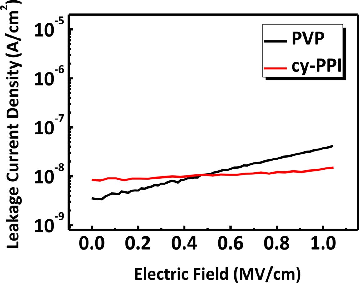
The leakage current of a gate dielectric layer should be as low as possible because it has a significant impact on the electrical performances of devices such as off current.27 Typical traces of leakage current density as a function of electric field strength are plotted for the cy-PPI and PVP films in Figure 7. The leakage current density of cy-PPI was maintained at about 10 nA/cm2 from 0 to 1 MV/cm. In contrast, the leakage current density of PVP increased significantly as the electric field strength was increased in this same range, and reached a value of 50 nA/cm2 at 1MV/cm.
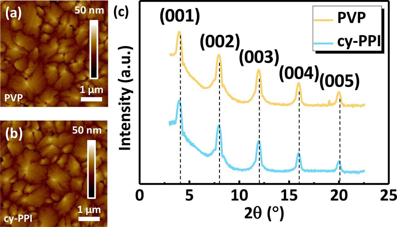
Organic Semiconductor Growth and Morphology on Gate Dielectric Films. Figure 8 shows the AFM images (5 μm×5 μm) of pentacene grown on optimized PVP and cy- PPI films. The pentacene grains on both films were large (average grain sizes of about 1200 nm) and well-connected to each other. The surface energy levels of the gate dielectrics may have affected the mode of growth of the pentacene molecules. 28 As indicated in the previous section, the surface properties of PVP and cy-PPI were almost the same. Therefore, it is reasonable to conclude that growth modes of the pentacene molecules on both films were the same, too. Generally, a large grain size for a semiconductor crystal gives a low number of grain boundaries that may act as carrier traps. All samples displayed (00l) patterns indicating that the ab planes of the pentacene crystals were oriented parallel to the substrate. Pentacene crystals deposited onto each substrate grew well into thin-film phases. The semiconductor crystal growth is directly affected by the dielectric surface properties; however, because the surface properties of the two different gate dielectrics were very similar, the XRD peak intensities were similar for the two systems. These results indicated that no poorly grown pentacene crystals, i.e., that would have formed a bulk phase crystal morphology and provided a barrier to charge carrier transport, were found on the gate dielectric surface.29 Due to no significant differences between the PVP and cy-PPI films, we concluded that the surface properties and semiconductor crystal growth did not seem to be having much an effect on the dielectric properties and electrical properties.
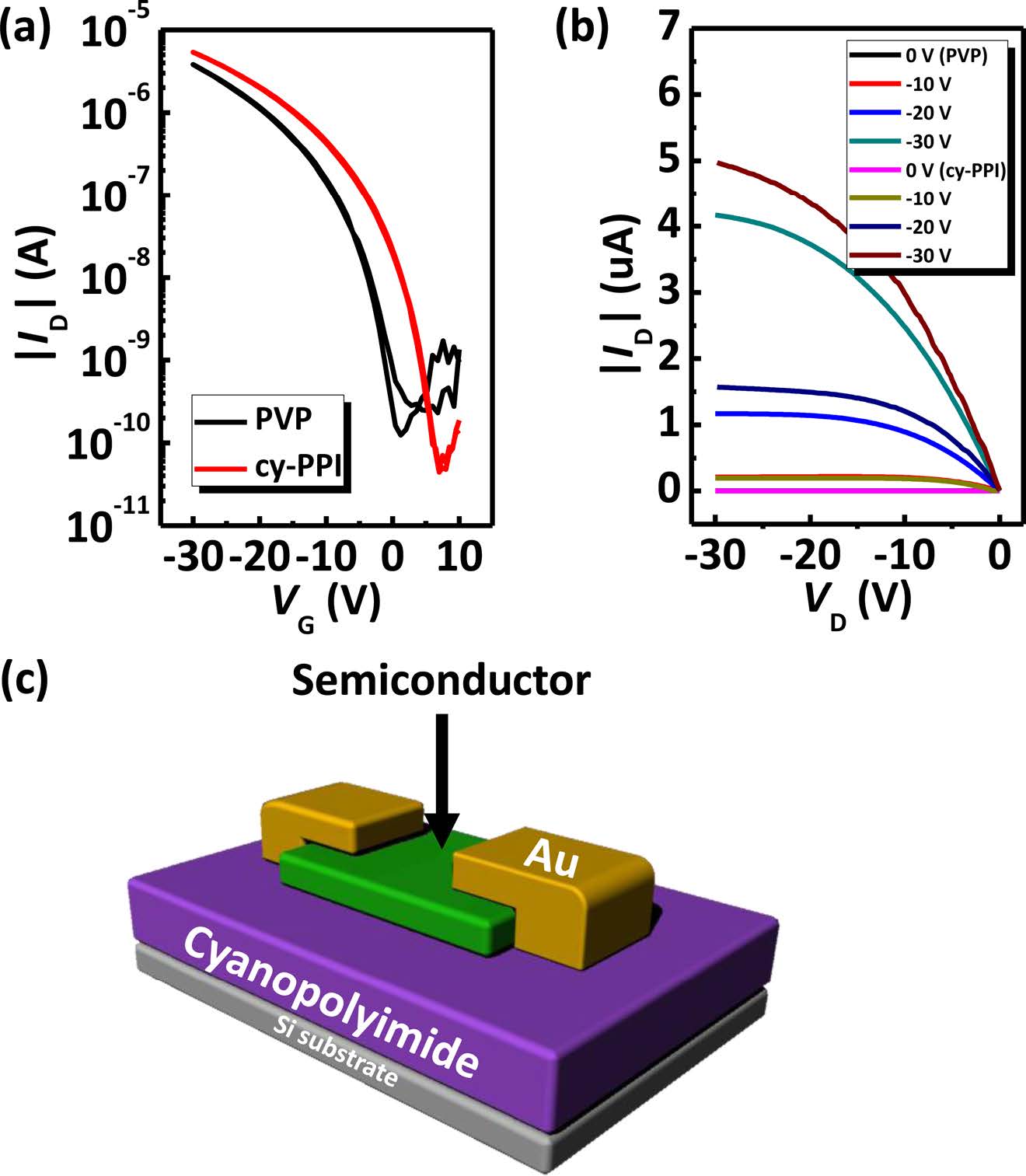
Electrical Characterization. To demonstrate the potential use of cy-PPI as a gate dielectric layer in OFETs, we fabricated a pentacene-based device. Figure 9 shows transfer and output characteristics of pentacene OFET devices based on cy-PPI and a schematic images of the prepared OFET device in this study. For securing reliability, more than 30 pentacene devices were tested in this study. In pentacene TFTs with a cy-PPI gate dielectric, charge carrier mobility, Vth, on/off ratio and SS were measured to be 0.15 cm2/Vs, -5.02 V, 1.2×10⁵, and 1.94 V/ decade, respectively. On the other hand, those values of pentacene with the PVP gate dielectric were 0.12 cm2/Vs, -10.58 V, 3.0×10⁴, and 2.12 V/decade, respectively. Average device electrical performances are also summarized in Table 2. The cy- PPI-based TFTs showed an overall better electrical performance than did the PVP-based TFTs. Hysteresis effects were negligible and gate leakage current was lower by several orders of magnitude than the source - drain current (< 10-8 A). Figure 9(b) shows the output characteristic curves of the cy- PPI, and PVP device; it exhibited typical p-type characteristics.
There are many reports indicating that SAMs terminated with electron-withdrawing groups on SiO2 gate dielectrics could accumulate holes in the transistor channels of pentacene TFTs. The accumulated holes would become additional mobile carriers, and therefore field-effect mobility can increase.30 Pentacene films on both PVP and cy-PPI films have been observed to display similar gate dielectric surface energy values and similar morphologies. Nevertheless, higher mobility and on/off ratio values were obtained from cy-PPI based TFTs. Electron-withdrawing groups on gate dielectrics can increase the work function of the semiconductor/gate dielectric interface more than not. As a result, in the gate dielectrics with an electron-withdrawing group, the band bending of the gate dielectric/semiconductor interface shifts toward higher energy and therefore more holes are accumulated at the interface.31 Thus, it can be concluded that lower leakage current level and strong electron-withdrawing groups of cy-PPI increase electrical performance.

|
Figure 1 Scheme of the synthesis of the poly(amic acid) (PAA). |
|
Figure 2 FTIR spectrum of the poly(amic acid) film. |

|
Figure 3 1H NMR spectrum of poly(amic acid) in dimethyl sulfoxide-D6. |
|
Figure 4 (a,b) AFM images; (c,d) water contact angle values of the (a,c) PVP and (b,d) cy-PPI films. |
|
Figure 5 UV-Vis spectrum of the cy-PPI film. |
|
Figure 6 Dielectric constant κ versus frequency for PVP and cy-PPI films at 25℃. |
|
Figure 7 Leakage current density of PVP and cy-PPI films with respect to electric field strength. |
|
Figure 8 (a,b) AFM images; (c) XRD patterns (out-of-plane) of pentacene on (a,c) PVP and (b,c) cy-PPI films. |
|
Figure 9 (a) Transfer characteristics (VG = 10 ~ -30 V, VD = -30V); (b) output characteristics (VG = -30V, VD = 0 ~ -30V); (c) a schematic diagram of the OFETs described in this report. |
We synthesized cyanated PI poly(2-cyano-p-phenylene pyromellitimide) (cy-PPI) as a gate dielectric material for OFETs. Introducing cyano groups helped the PI to be dissolved in solvent, and hence be available for solvent process, by reducing the interactions between PI chains. Transmittance greatly improved in the visible wavelength range. The cy-PPI films showed no pin-holes, and had smooth surfaces enough to grow semiconductor molecules well. They exhibited good capacitance stability regardless of frequency, and low leakage current density compared to the conventional organic gate dielectric, i.e., PVP. To further analyze the electrical performance, we performed AFM and XRD analyses, and confirmed that pentacene semiconductor molecules were well-grown on the cy-PPI gate dielectric surface. Based on these results, we fabricated OFET devices each with a cyanated PI film as the gate dielectric. Being one of the strongest electron-withdrawing groups, cyano groups of the gate dielectrics attracted additional holes into the channel. Thus, compared to the PVP gate dielectrics, our cy-PPI OFETs showed a better overall electrical performance (0.15 cm2/Vs (hole mobility), -5.02 V (threshold voltage), 1.2×10⁵ (on/off ratio), and 1.94 V/decade (subthreshold slope)). To the best of our knowledge, this is the first report of the study of the potential of cyanated PI for use in OFET applications.
- 1. X. Ren, K. Pei, B. Peng, Z. Zhang, Z. Wang, X. Wang, and P. K. Chan, Adv. Mater., 28, 4832 (2016).
-

- 2. W. Lee, D. Kim, J. Rivnay, N. Matsuhisa, T. Lonjaret, T. Yokota, H. Yawo, M. Sekino, G. G. Malliaras, and T. Someya, Adv. Mater., 28, 9722 (2016).
-

- 3. K. Kim, J. Bae, S. H. Noh, J. Jang, S. H. Kim, and C. E. Park, J. Phys. Chem. Lett., 8, 5492 (2017).
-

- 4. N. Cui, H. Ren, Q. Tang, X. Zhao, Y. Tong, W. Hu, and Y. Liu, Nanoscale, 10, 3613 (2018).
-

- 5. Y. Wang, X. Huang, T. Li, Z. Wang, L. Li, X. Guo, and P. Jiang, J. Mater. Chem. A, 5, 20737 (2017).
-

- 6. T. Yokota, P. Zalar, M. Kaltenbrunner, H. Jinno, N. Matsuhisa, H. Kitanosako, Y. Tachibana, W. Yukita, M. Koizumi, and T. Someya, Sci. Adv., 2, e1501856 (2016).
-

- 7. H. Phan, M. J. Ford, A. T. Lill, M. Wang, G. C. Bazan, and T. Q. Nguyen, Adv. Funct. Mater., 27, 1701358 (2017).
-

- 8. Y. Baek, S. Lim, L. H. Kim, S. Park, S. W. Lee, T. H. Oh, S. H. Kim, and C. E. Park, Org. Electron., 28, 139 (2016).
-

- 9. S. H. Kim, H. Yang, S. Y. Yang, K. Hong, D. Choi, C. Yang, D. S. Chung, and C. E. Park, Org. Electron., 9, 673 (2008).
-

- 10. Y. Wang, T. Hasegawa, H. Matsumoto, T. Mori, and T. Michinobu, Adv. Mater., 30, 1707164 (2018).
-

- 11. A. Facchetti, M. H. Yoon, and T. J. Marks, Adv. Mater., 17, 1705 (2005).
-

- 12. P. H. Chu, G. Wang, B. Fu, D. Choi, J. O. Park, M. Srinivasarao, and E. Reichmanis, Adv. Electron. Mater., 2, 1500384 (2016).
-

- 13. W. Huang, H. Fan, X. Zhuang, and J. Yu, Nanoscale Res. Lett., 9, 479 (2014).
- 14. W. S. Machado and I. A. Hummelgen, IEEE Trans. Electron. Devices, 59, 1529 (2012).
- 15. K. Sethuraman, S. Ochiai, K. Kojima, and T. Mizutani, Appl. Phys. Lett., 92, 162 (2008).
- 16. Y. Yun, C. Pearson, and M. C. Petty, J. Appl. Phys., 105, 034508 (2009).
- 17. X. Cheng, M. Caironi, Y.-Y. Noh, J. Wang, C. Newman, H. Yan, A. Facchetti, and H. Sirringhaus, Chem. Mater., 22, 1559 (2010).
-

- 18. K. Vanherck, G. Koeckelberghs, and I. F. Vankelecom, Progr. Polym. Sci., 38, 874 (2013).
-

- 19. S. H. Hsiao, H. M. Wang, W. J. Chen, T. M. Lee, and C. M. Leu, J. Polym. Sci., Part A: Polym. Chem., 49, 3109 (2011).
-

- 20. A. Ghosh, S. K. Sen, S. Banerjee, and B. Voit, RSC Adv., 2, 5900 (2012).
-

- 21. H.-j. Ni, J.-g. Liu, Z.-h. Wang, and S.-y. Yang, J. Ind. Eng. Chem., 28, 16 (2015).
-

- 22. L. Zhai, S. Yang, and L. Fan, Polymer, 53, 3529 (2012).
-

- 23. S. D. Kim, S. Y. Kim, and I. S. Chung, J. Polym. Sci., Part A: Polym. Chem., 51, 4413 (2013).
-

- 24. G. Zhang, H.-h. Ren, D.-s. Li, S.-r. Long, and J. Yang, Polymer, 54, 601 (2013).
-

- 25. W. Shao, H. Dong, L. Jiang, and W. Hu, Chem. Sci., 2, 590 (2011).
-

- 26. S. H. Kim, W. M. Yun, O.-K. Kwon, K. Hong, C. Yang, W.-S. Choi, and C. E. Park, J. Phys. D: Appl. Phys., 43, 465102 (2010).
- 27. H. Moon, H. Seong, W. C. Shin, W.-T. Park, M. Kim, S. Lee, J. H. Bong, Y.-Y. Noh, B. J. Cho, and S. Yoo, Nat. Mater., 14, 628 (2015).
- 28. S. Y. Yang, K. Shin, and C. E. Park, Adv. Funct. Mater., 15, 1806 (2005).
-

- 29. S. H. Kim, M. Jang, H. Yang, and C. E. Park, J. Mater. Chem., 20, 5612 (2010).
-

- 30. K. Pernstich, S. Haas, D. Oberhoff, C. Goldmann, D. Gundlach, B. Batlogg, A. Rashid, and G. Schitter, J. Appl. Phys., 96, 6431 (2004).
-

- 31. Y. Jang, J. H. Cho, D. H. Kim, Y. D. Park, M. Hwang, and K. Cho, Appl. Phys. Lett., 90, 132104 (2007).
- Polymer(Korea) 폴리머
- Frequency : Bimonthly(odd)
ISSN 0379-153X(Print)
ISSN 2234-8077(Online)
Abbr. Polym. Korea - 2023 Impact Factor : 0.4
- Indexed in SCIE
 This Article
-
2019; 43(1): 38-45
Published online Jan 25, 2019
- 10.7317/pk.2019.43.1.38
- Received on Jun 25, 2018
- Revised on Sep 7, 2018
- Accepted on Sep 19, 2018
 Services
- Full Text PDF
- Abstract
- Acknowledgements
Introduction
Experimental
Results and Discussion
Conclusions
- References
Shared
 Correspondence to
- Sung Soo Han**, Tae Kyu An*** , and Se Hyun Kim**
-
**School of Chemical Engineering, Yeungnam University, Gyeongsan 38541, Korea
***Department of Polymer Science & Engineering and IT Convergence, Korea National University of Transportation, 50 Daehak-Ro, Chungju 27469, Korea - E-mail: sshan@yu.ac.kr, taekyu1985@ut.ac.kr, shkim97@yu.ac
- ORCID:
, 0000-0002-2130-1561, 0000-0001-7818-1903


 Copyright(c) The Polymer Society of Korea. All right reserved.